
The performance of photovoltaic solar cells is hinged on the amount of solar energy absorbed by the active layer of the solar cell. The amount of light energy transmitted through the top cover of the solar cell determines how much of the light energy is absorbed by the solar cell [1,2]. The solar cell’s top cover significantly influences the transmission of incident radiation into the solar cell. However, not all the light that is incident is transmitted and consequently absorbed, but a fraction is lost through reflection and scattering, which ultimately lowers the cell’s efficiency [3].
Therefore, it is very vital to fabricate nanostructures that have high transmittance but low reflectance to short-wavelength ultraviolet, visible, and near-infrared radiations [4,5]. Although single layer antireflection coatings have been demonstrated, double- or multiple-layer dielectric thin films are being adopted to attenuate the intensity of light energy reflected by the solar cell [6,7].
In the recent past, [8] used magnetron sputtering to prepare ZnS thin films on glass. The transmittance was predominantly low, and it ranged between 63.0% and 95.7% in the visible spectrum. Furthermore, [9] used magnetron sputtering to coat ZnS thin films on bare polycrystalline silicon cell and obtained an average transmittance of 90%. The zinc sulphide was used because of its high refractive index (2.35) and wide band gap (3.7 eV), which reduce absorption losses in the short wavelength spectrum and thus improve short-circuit current.
Relatedly, [10] characterised Al\(_2\)O\(_3\) thin films prepared by magnetron sputtering at different sputtering powers and argon pressures. Transmittance values of 92% to 94% were obtained, while the reflectance values ranged from 7% to 10%. The Al\(_2\)O\(_3\) was selected because it is stable and does not easily degrade in the environment [11,12]. Secondly, Al\(_2\)O\(_3\) has a high band gap of 5.1-8.8 eV for different crystallographic structures [].
The transmission and reflection processes occurring in the double layers produce either constructive and/or destructive interference effects. Destructive interference is of great importance in the design of antireflection nanofilms. Destructive interference occurs when the incident light energy is reflected out of phase by \(180^o\) into the incident medium [14]. The phenomenon of destructive interference is influenced by several factors ranging from film thickness, microstructure, film density, and surface morphology. However, the energy changes that take place on the front cover of the solar cell [15] are governed by the relation: \[T+R+A=1, \tag{1}\] where \(A\), \(T\), and \(R\) are the absorbance, transmittance, and reflectance [16]. The amount of reflection that occurs due to refractive index change at an interface at normal incidence [17,18] is defined by the equation: \[R=\left(\frac{n_{p}-n_{m}}{n_{p}+n_{m}}\right)^2, \tag{2}\] where \(n_p\) is the refractive indices of the thin film and and \(n_m\) is the refractive index air [17]. The amount of light energy transmitted \(T\), through a material of thickness \(t\), is calculated from the reflectance \(R\) and absorption coefficient \(\alpha\) of the transmitting material as follows: \[T=\frac{1}{t}\frac{\ln(1-R)^2}{\alpha}. \tag{3}\] Thus, in this work, we demonstrate the effect of deposition time, sputtering power, and argon and oxygen flow rate on the spectral transmittance of Al\(_{2}\)O\(_{3}\) and ZnS:Cu antireflection nanostructures.
The indium tin oxide substrate was cleaned in an ultrasonic bath containing a solution of sodium stearate soap for 15 minutes and later rinsed with distilled water, ethanol, and acetone for ten minutes. The substrates were then dried in the air using argon gas. The substrates were then placed 14 cm vertically above the target in the vacuum chamber. The Edwards 306 magnetron sputtering machine was used for the preparation of thin films [19,20]. Radiofrequency sputtering was used for the deposition of copper-doped zinc sulphide ZnS:Cu (94/6.0% copper) onto the substrate using argon (99.9% pure) as a working gas. The argon gas flow rates used were 40, 70, and 100 sccm. The radio frequency sputtering power values of 70 W, 100 W, and 140 W were also used at a low process pressure of \(6.5 \times 10^{-3}\) for 5, 10, 20, and 30 minutes.
Direct current (D.C.) reactive sputtering was used for the deposition of aluminium oxide using the aluminium (Al) target (99.99% purity) and oxygen (99.9% pure). The chamber was pumped down to a high vacuum of \(5.5 \times 10^{-5}\) mBar before sputtering was allowed to take place. The process proceeded by allowing oxygen gas into the chamber at gas flow rates of 40, 70, and 100 sccm. The D.C. power values of 70 W, 100 W, and 140 W were used. The D.C. sputtering was allowed to take place at a low process pressure of \(6.5 \times 10^{-3}\) mBars for 5, 10, 20, and 30 minutes. The high-energy oxygen ions hit the Al target, causing target atoms to break off to form aluminium vapour [21]. The oxygen ions react with Al atoms to form Al\(_{2}\)O\(_{3}\) [22,23] vapour, which is transported to the substrate.
The Al\(_{2}\)O\(_{3}\) films were deposited onto the ZnS:Cu/ITO substrate to form the Al\(_{2}\)O\(_{3}\)/ZnS:Cu/ITO double-layer structure. In both methods, the target-to-substrate distance was set to 14 cm. The flow of argon and oxygen gases was controlled by the Alicat Scientific (MC-100SCCM-D/5M, 5IN) (Tucson, AZ, USA), and the samples were uniformly rotated by a rotary workholder connected to the rotary workholder drive. After the Al\(_{2}\)O\(_{3}\)/ZnS:Cu films had been deposited, the samples were removed from the vacuum chamber and kept in an incubator containing calcium oxide. The sample’s thickness was then measured by the Alpha-Step IQ surface profiler by taking measurements at three different points across the length of the film. An average value of film thickness was computed and recorded.
The samples’ transmittance and reflectance were measured by the spectrophotometer, model Solidspec-3700 DUV, in the wavelength range of 200 to 800 nm. The microstructure of the samples was studied by the x-ray diffractometer machine, ARL Equinox 100. The copper anode (Cu K\(_{\alpha}\) radiation) was used with an x-ray emission wavelength of 1.54056 Å with a scan time of 240 s. The film roughness was studied by the scanning electron microscope (SEM) (model ZEISS) operating at 6.00 kV, WD of 9.6 mm, and signal A = SE2. The samples were analysed after sample treatment with chromium as the electron-conducting material.
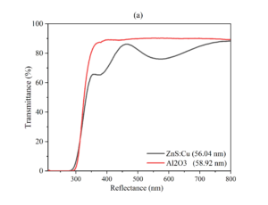
The transparent single-layer Al\(_{2}\)O\(_{3}\) and ZnS:Cu nanostructures formed with different film thicknesses have been analysed as shown in Figure 1(a). The transmittance of the nanofilms increased from the short-wavelength ultraviolet band toward the long-wavelength visible spectrum. However, interference effects observed in the ZnS:Cu films were due to reflections from the film and substrate interfaces [24]. This is because highly crystallised nanostructures exhibit fewer defects [25], grain boundaries, and structural imperfections, which reduces the scattering of light energy. This effect enhances the transmittance of visible light [9,26].
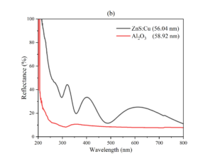
To visualise how much of the incident energy was reflected, the reflectance characteristics of Al\(_2\)O\(_3\) and ZnS:Cu are presented in Figure 1(b). The reflectance of ZnS:Cu(56.04 nm) was recorded to be 11.94% at the wavelength \(\lambda=488\) nm. Interference effects were observed in the reflectance spectra of ZnS:Cu(56.04 nm). The reflectance of Al\(_2\)O\(_3\)(58.92 nm) thin films was 7.19%. The recorded reflectance values are relatively high. Moreover, [27] argued that the shortcomings of a single-layer antireflection coating include the reduction in reflectance over limited wavelengths [28].
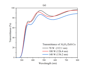
The transmittance of single-layer ZnS:Cu nanostructures (Figure 2(a)) was observed to decrease with an increase in sputtering power. An absorption edge in the ultraviolet region with a red shift in the fundamental absorption edge, which increased with sputtering power and film thickness. Furthermore, at the absorption edge, the transmittance for different sputtering powers is 73.49%, 66.86%, and 69.43% for 70 W, 100 W, and 140 W, respectively. The transmittance of Al\(_2\)O\(_3\) nanostructures (Figure 2(b)) was observed to increase from the short wavelength towards the long wavelength part of the electromagnetic spectrum.
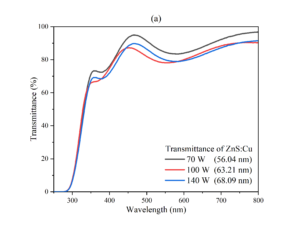
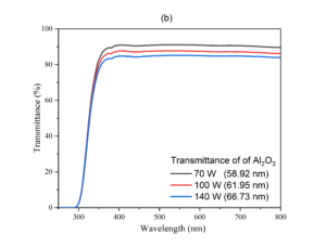
The highest transmittance of 91.45%, 88.14%, and 85.20% was obtained for the films sputtered at 70 W, 100 W, and 140 W, respectively. A related study by [10] on the optical properties of Al\(_2\)O\(_3\) gave maximum transmittance of 92% and reflectance of approximately 7.8%. However, low deposition power results in a slow deposition rate, leading to small film thickness with lower density, which increases the scattering of light energy. At higher sputtering power, the films form a dense and uniform microstructure, which decreases transmittance [29,30]. Therefore, based on the transmittance data discussed in this section, the single-layer nanostructures will require modification to lower the transmittance of light energy in the entire electromagnetic spectrum.
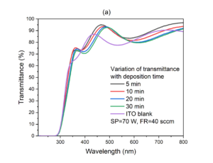
The transmittance spectra for the transparent Al\(_2\)O\(_3\)/ZnS:Cu thin nanofilms are shown in Figures 3. An increase in the deposition time increased the transmittance because the substrate receives more ionised atoms for deposition, hence an increase in film thickness [31]. The transmittance of the ITO blank was generally lower than for the coated films. This shows an improvement in the transmission characteristic of the Al\(_2\)O\(_3\)/ZnS:Cu nanostructures [32]. The highest the transmittance values ranged between 72 and 98%, which highlight good antireflection properties. The high transmission was due to reduced scattering and micro defects in the nanostructures [33,34] and high film homogeneity.
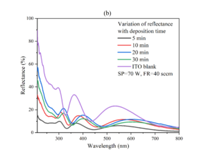
A comparative study of the reflectance of Al\(_2\)O\(_3\)/ZnS:Cu thin nanofilms deposited at a sputtering power of 70 W is presented in Figure 3(b). The reflectance of Al\(_{2}\)O\(_{3}\)/ZnS:Cu nanostructure increased with an increase in deposition time. This reciprocal behaviour in transmittance and reflectance satisfies the energy balance condition of equation (1.1), assuming there is no absorption in the thin films [14,16]. The effective reflectance of the nanostructures decreased significantly and approached minimum values of 3.03% to 4.61% in the ultraviolet region and 9.08% to 11.38% in the visible region. The shape of the reflectance curve, according to [35], corresponds to the requirement for a well-matched refractive index gradient. This spectral behaviour was also observed by [27] and [35].
The variation of transmittance with sputtering is presented in Figure 4(a). The transmittance gradually decreased as the power was raised from 70 W to 140 W. At low sputtering power, in the presence of the sputtering gas, the sputtered ions were thermalised by collision during the transition to the substrate. Therefore, less energetic ions can hardly diffuse across the surface of the substrate, resulting in poor crystallinity in the growing film [36]. When the sputtering power was raised, the sample’s film thickness increased due to the high rate of deposition [37], which increased the grain size of the nanofilms. This makes the surface rough and results in the enhanced scattering of light energy. This is the reason for the observed decrease in the transmittance as the sputtering power increases [38].
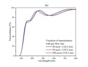
In Figure 4(b), the transmittance curves for different flow rates increased from the short wavelength to the long wavelength with overlaps in intensity at different wavelengths. Nonetheless, the effect of gas flow rate did not have a clear-cut effect on the transmittance of the nanostructures due to overlaps along the spectrum. However, an increase in gas flow rate causes high collision rates between the gas molecules and sputtered ions. This can result in rougher or more porous films, which can scatter light, thus decreasing the optical transmittance. Additionally, high flow rates may introduce more impurities or contaminants into the film, further reducing transmittance [39,40].
The microstructure of Al\(_{2}\)O\(_{3}\)/ZnS:Cu nanofilms formed at different argon and oxygen flow rates is shown in Figure 5. The crystallite size of the samples was calculated by the modified Scherrer formula [41] according to: \[\ln \beta = \ln\left(\frac{K\lambda}{D_{hkl}}\right) + \ln\left(\frac{1}{\cos\theta}\right). \tag{4}\] The acceptable intercept is obtained when the \(slope \approx 1\).
When a graph of \(\ln\beta\) was plotted against \(\ln(\frac{1}{\cos\theta})\) a straight line was obtained with an intercept \(c\) equal to \(\ln\frac{K\lambda}{D_{hkl}}\) along the \(\ln\beta\) axis [42]. The shape factor, \(k \approx 0.9\), \(D_{hkl}\) is the crystallite size, \(\lambda\) is the wavelength of x-rays, \(\theta\) is the diffraction angle, and \(\beta\) is the full width at half maximum (FWHM) of the diffraction peak [43]. It was noted that all the multilayers are crystalline with strong peak intensities located between \(2\theta =25.43^o\) and \(36.44^o\). A strong peak for the (220) crystallographic plane belongs to ZnS according to ICSD card number 67453.
This peak appears in nanofilms formed during the gas flow rates of 40 sccm and 70 sccm. This plane reveals cubic ZnS structure, which was also reported by [33] according to card number: PDF 05-0566. Another dominant peak of (221) was assigned to Al\(_{2}\)O\(_{3}\) crystallographic planes according to ICSD CODE 9770. These planes were preferred because their formation energy was lower than the surface energy of other lattice planes [44,45]. However, Cu-related diffraction peaks from ZnS:Cu were not observed in the XRD patterns. This is because the copper (II) ions only act as foreign particles in the ZnS lattice, in which the cooper (II) occupy Zn sites in the ZnS lattice. This similar behaviour was reported by [33].
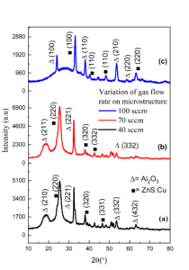
The changes in peak intensities had a proportionate decrease in the crystallite size from 0.02508 to 0.02071 Å, Table 1. Separate studies by [46] and [47] revealed that the decrease in crystallinity and hence grain size of the crystallites was attributed to the increase in the argon and oxygen gas flow rates. Further explanation by [39] asserts that an increase in argon flow rate increases the background pressure of the gas, which consequently decreases the rate of film growth.
This observation was earlier explained by [48] that at long target substrate distances, the high-velocity argon atoms tend to take away low-energy sputtered atoms. This implies that some of the low-energy atoms are less likely to reach the substrate, thus making the growth rate drop as the flow rate increases [49]. The crystallite sizes of the samples were analysed by the modified Scherrer formula: \[\ln \beta = \ln\left(\frac{K\lambda}{D_{hkl}}\right) + \ln\left(\frac{1}{\cos\theta}\right). \tag{5}\]
Plotting a graph of \(\ln\beta\) against \(\ln(\frac{1}{\cos\theta})\) gives a straight line with an intercept \(c\) equal to \(\ln\frac{K\lambda}{D_{hkl}}\) along the \(\ln\beta\) axis [42]. The shape factor, \(k \approx 0.9\), \(D_{hkl}\) is the crystallite size, \(\lambda\) is the wavelength of x-rays, \(\theta\) is the diffraction angle of a particular diffraction peak, and \(\beta\) is the full width at half maximum (FWHM) of the diffraction peak corresponding to a given crystal plane [43].
| GFR (sccm) | \(2\theta\) | d ()Ä | FWHM \((^o)\) | D\(_hkl\) (nm) | \(\delta\) (nm\(^-2\)) |
| 40 | 27.18 | 2.795 | 3.116 | 0.02508 | 1589.8 |
| 70 | 25.47 | 2.675 | 3.370 | 0.02278 | 1927.0 |
| 100 | 25.47 | 2.621 | 3.831 | 0.02071 | 2331.5 |
When the increase in gas flow rate was raised, the FWHM also increased which indicates that the crystallinity of the films was deteriorating, and hence, the crystallite size of the Al\(_{2}\)O\(_{3}\)/ZnS:Cu nanoparticles decreased with an increase in the gas flow rate. According to [50] and [51], the decrease in crystallite size was due to defects or dislocations generated during film formation. This trend was also reported by [52]. The lattice parameter \(d\) for crystallite structure for different flow rates was calculated from the Bragg’s law equation [40,53].
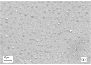
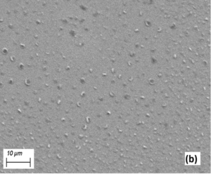
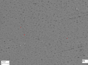
The morphological images of transparent Al\(_2\)O\(_3\)/ZnS:Cu nanostructures sputtered with argon and oxygen flow rates of 40, 70, and 100 sccm are shown in Figure 6. The Al\(_2\)O\(_3\)/ZnS:Cu nanofilms were found to be continuous and dense. At a low gas flow rate of 40 sccm (Figure 6(a)), the Al\(_2\)O\(_3\) and ZnS:Cu particles are uniformly distributed over the surface of the substrate. There is a decrease in crystallinity due to the reduced number of atoms migrating on the surface of the substrate. This is because an increase in gas flow rate reduces the mean free path of the sputtered ions and hence increases the number of ions in the plasma [39]. This increases the probability of interionic collisions that result in the reduction of the number of ions per second reaching the substrate. Nonetheless, further increase in gas flow rate to 100 sccm led to the non-uniform distribution of sputtered particles on the substrate’s surface. This is because during the deposition, agglomerations of both Al\(_2\)O\(_3\) and ZnS:Cu are formed as a result of the low rate of nucleation on the surface of the substrate [9].
The transmittance spectra data for the Al\(_2\)O\(_3\) and ZnS:Cu nanostructures show single-layer nanostructures had lower transmittance values than double-layer nanostructures. Double-layer nanostructures had above-average transmittance values (68.11% to 75.44%) in the ultraviolet region and the highest transmittance (78.85% and 96.63%) in the visible region. However, the transmittance was observed to decrease with an increase in sputtering power and deposition time. The low values of reflectance are highly commendable for photovoltaic antireflection nanostructures. The effective reflectance of the nanostructures decreased significantly and approached minimum values of 3.03% to 4.61% in the ultraviolet region and 9.08% to 11.38% in the visible spectrum. The nanostructures are crystalline with strong peak intensities located at \(2\theta=25-43^o\). Nonetheless, the crystallite sizes decreased from 0.02508 to 0.02071 Å as the gas flow rate increased from 40 to 100 sccm. This decrease in crystallinity was due to the reduced number of atoms migrating on the surface of the substrate. The morphology of the deposited ZnS:Cu films was found to be smooth, continuous, and dense. The results demonstrate that the double-layer Al\(_2\)O\(_3\) and ZnS:Cu nanostructures are highly commendable for use as antireflection materials for the top cover photovoltaic solar cells.