This paper presents the spectral reflectance of thermally evaporated ZnS/Ag nanostructures. The coating of ZnS/Ag nanostructures was performed in two steps while varying the film thickness and deposition angle. Silver metal wire (99.99% purity) was heated under vacuum at a pressure of \(2.5 \times 10^{-5}\) mBars and deposited on glass slide substrates in the diffusion pump microprocessor vacuum coater (Edwards AUTO 306). Pieces of zinc sulphide (99.99% purity) were heated and deposited to the glass slides previously coated with silver to form the ZnS/Ag/glass composite. The optical reflectance of the samples was studied by the UV/Vis/NIR spectrometer (Perkin Elmer Lambda 19) with UV-WinLab software. The reflectance was measured at angles of incidence between \(15^o\) and \(75^o\). Spectrophotometric studies showed that reflectance decreased with decrease in film thickness and decreased with increase in deposition angle of silver nanoparticles. The reflectance of ZnS/Ag nanostructures decreased with increase in deposition angle of zinc sulphide.
The reflectance properties of surfaces of optical components in several devices in use today require careful tailoring to meet the requirements of technological advances. Reflective mirrors for use in domestic and industrial housing units in hot climates should have the potential to reflect a high percentage of infrared radiation but transmit a desirable amount of visible light. However, these reflective surfaces are susceptible to environmental degradation. This is a fundamental setback in optical applications. It is very vital for the reflective surfaces to be protected and made resistant to weather and chemicals in the environment [1,2]. Most reflective mirrors are coated with metals films such as silver, copper, gold, aluminium to improve there reflective characteristics. These metals at nano-scale have remarkably low optical absorption in the visible region and high reflectance in the infrared region and frequency dependent refractive index [3,4,5]. The additional technical characteristic of silver at nano-scale is that of high chemical and optical activity with the capacity to fuse with dielectric materials to form hybrid semiconductor layers [6,7,8].
Nevertheless, whenever materials such as silver, gold, copper, and aluminium are exposed to the environment, they tend to age out due to environmental degradation. They thus have to be protected by coating them with a suitable material in form of a transparent dielectric coating material. A dielectric material is a transparent film which has strong ionic or directed covalent bonds. Most dielectrics are transparent to visible and/or infrared light. When an electromagnetic radiation falls on a dielectric material, it interacts with valency band electrons. The valency band electrons absorb energy and under go electronic transitions to the conduction band. This changes the the optical parameters of the dielectric films [9,10]. The change in optical properties can be quantified by solving Maxwell equations at the boundary between different optical media subject to boundary conditions [10]. Dielectrics used for this purpose include zinc oxide, magnesium floride, zinc sulphide, indium tin oxide among others [11,12]. The optical characteristics of zinc oxide, magnesium floride, zinc sulphide, indium tin oxide are among other factors governed by deposition conditions which include deposition pressure, temperature, deposition rate and deposition angle [13]. Other factors like film thickness are required when tuning the spectral reflective properties of nanostructured components for optical, electrooptic, telecommunications and architectural applications in energy conservation [14].
The energy efficiency of buildings for residential and industrial storage facilities in most instances is regulated with external cooling mechanisms such as electric powered air conditioners. The cooling systems are very expensive to maintain on the short and long run. The architectural windows and doors are part of the alternative natural cooling options that are cheap to install and maintain. Several buildings are fitted with float glass windows whose spectra properties have not been quantified by any spectrophotometric processes. However, glass panes used on windows should be designed to reflect infrared radiation but at the same time allow a considerable amount of visible light to pass through them. On this note, the optical structural adjustment of the window surface has always not been a simple task to under take [15,16,17]. Many attempts have been made to modify the optical properties of glass by applying transparent polystyrene or coating the glass surface with transparent dielectric or metallic thin films. During thin films deposition processes, it is vital to control the vapour flux coming from evaporating materials. The evaporating material may reach the substrate normally or at an oblique angle. At normal incident, the vapour flux upon deposition tends to form a relatively uniform homogeneous film. Nevertheless, the growth of very thin films is always accompanied by the formation of atomic islands on the surface of the dielectric [18,19].
However, during oblique deposition, the adhesion of initial particles on the substrate may hinder the direct impact of preceding atoms on the substrate. Along the direction of initially deposited atoms, columns are formed that shadow the incoming vapour atoms from reaching directly to the substrate surface [20,21]. This leads to the formation of columner structures which restrict adatom mobility and surface diffusion of deposited particles. Oblique deposition therefore, produces rough surfaces but also changes film micro-structure [22,23]. Atomic islands are also formed for very thin nanostructures (\(< 12\) nm) [24]. The microstructure may have pores or internal voids that affect the density, optical reflectance, transmittance and optical absorbance of the thin films [25,26].
When an electromagnet radiation is incident on a thin film coated on glass surfaces, it is either transmitted with attenuation or upon reflection may surfer interference effects due multiple reflections from different media interfaces. However, the extent of these effects depend on the values of optical constants, angle of incidence, microstructure and surface roughness of the reflective surface. Additionally, reflectance of a surface may be affected by the relative motion between the Earth and the Sun. The intensity of electromagnetic radiation from the Sun changes with time along side other factors like, location, the Sun angle and solar shading. Hence, it is very important to measure and establish the reflectance values for different angles of incident radiation for every reflecting surface. This information is very important in structural design of fenestration especially transparent windows and doors [27]. Although several attempts have been made to control thermal conductivity through walls and the roof of buildings [28,29], thermal radiation transfer from the ambient through the transparent windows and doors into the building envelope remains one of the biggest challenges in the housing industry. Thus in this paper, the authors present the spectral reflectance of ZnS/Ag nanostructures hinged on film thickness, deposition angle and angle of incidence of electromagnetic radiation.
The deposition of ZnS/Ag thin films was performed in two steps while varying the film thickness and deposition angle. Silver metal wire (99.99% purity) was heated on a refractory tantalum boat under vacuum at a pressure of \(2.5 \times 10^{-5}\) mBars and deposited on glass slide substrates in the diffusion pump microprocessor vacuum coater (Edwards AUTO 306). The heating current was slowly raised to a current of 38 A because silver metal has low melting point of 961\(^o\)C. The evaporation rate of 1 nms\(^{-1}\) was used. Glass slides were fixed on a rotary holder placed 11 cm away from the refractory boat vertically above it. The substrate holder together with the glass slide was rotated at an angle \(\theta\) about the horizontal so that the vapor is incident at an angle \(\theta\) to the substrate normal (the angle between the normal to the substrate and direction of incidence of the evaporated atoms). The setup is shown in Figure 1 below. Three sets of samples of silver films of thickness 4 nm were deposited at different angles of \(\theta= 0^o\), 30\(^o\) and 60\(^o\). This was repeated for each of thickness of 7, 10 and 15 nm onto glass substrate.
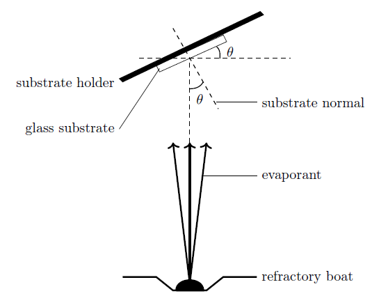
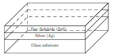
The pieces of ZnS (99.99% purity) were heated in a molybdenum boat with source cover to reduce the spreading of the vapor. Because ZnS has a high melting point of 1830\(^o\)C, the heating current was increased to 56 A. The ZnS was heated and deposited to film thickness of 4 nm at vapour incidence angle \(\theta = 0, 30\) and \(60^o\) to the glass slides previously coated with silver to form the ZnS/Ag/glass multilayer system shown in Figure 2.
This procedure was repeated for thicknesses 7, 10 and 15 nm. The thickness monitor was calibrated separately for each of the materials in the vacuum chamber. The thickness of the films were measured by a thickness monitor connected to a quartz crystal monitoring system placed inside the diffusion chamber [30]. In vacuum vapour deposition, it is very had to produce films that have perfectly smooth surfaces with high homogeneity and uniform thickness. This effect compromises the accuracy of the spectrophotometric results since the measurement of transmittance and reflectance can hardly be done at exactly the same spot on the specimen [31].
The optical reflectance of the samples were studied by the UV/Vis/NIR spectrometer (Perkin Elmer Lambda 19) with UV-WinLab software. This is a double beam instrument covering the ultraviolet, visible and near infrared spectral wavelength. Baseline measurement using a clean piece of substrate was done. Reflectance was measured at angles of incidence; 15\(^o\), 30\(^o\), 45\(^o\), 60\(^o\), and \(75^o\) of the incident radiation to the optical system in the wavelength range of 250 to 2500 nm [32]. Since it is very had to measure reflectance at normal incidence, the lowest angle of incidence for reflectance measurements was \(15^{o}\) subject to the limitations of the spectrometer model used [33].
The spectrophotometric measurements on reflectance was analysed on specimens fabricated with different thickness and deposition angles. The reflectance of normally deposited ZnS(0)/Ag(0) nanostructures was relatively low (ranged between 5% – 35%) in the visible range (400-780 nm) of the electromagnetic spectrum followed by a rise in reflectance towards the infrared at about \(\lambda = 800\) nm, Figure 3 (a). The reflectance results showed remarkable interference effects in the infrared region in all the samples. These effects were dependent on the film thickness and wavelength of the electromagnetic radiation. The interference effects ware observed in the infrared region 800-2200 nm and the tended to disappear or diminshed as the wavelength approached the the upper edge of the visible spectrum. This observation was also reported in the obliquely deposited Nb\(_2\)O\(_5\) [34] and ZnO [35] thin films.
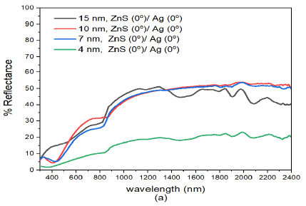
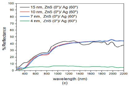
The interference effects in the infrared region were more intense in the (15 nm)ZnS(0)/Ag(0) nanostructures. These effects were as a result of reflection from different optical interfaces of air-ZnS, ZnS-Ag, and Ag-glass interfaces [36]. The interference effects infer that the prepared samples were relatively smooth and uniform [37,38]. There was a further rise in reflectance to about 54% in the infrared region at about \(\lambda = 1300\) nm. It was also observed that the reflectance decreased with decrease in film thickness of ZnS/Ag multilayer films Figure 3 (a). However, there was a big drop in reflectance with film thickness from (7 nm)ZnS(0)/Ag(0) to (4 nm)ZnS(0)/Ag(0). The decrease in reflectance was partly due to decrease in film thickness and formation of atomic islands during the deposition of very thin metal films and dielectric nanostructures [39,40].
For wavelength below \(\lambda =400\) nm, there were interference minima in reflectance of the samples. These effects according to Wlodarski et al., [41] and Zhou and Liu [42] were as a result of increase in absorption due to interband electronic transitions of the zinc and silver atoms. Thin nanostructures of (4 nm)ZnS(0)/Ag(0), had very low reflectance values i.e. between 2.6% – 10.5% in the visible region and reflectance increased to a maximum value of 22.1% at \(\lambda =2000\) nm in the infrared wavelength as shown in Figure 3 (a).
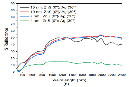
When the deposition angle of Ag nanoparticles was increased to \(30^o\) in the ZnS/Ag composite i.e. ZnS(0)/Ag(30) Figure 3 (b), the reflectance decreased progressively as the thickness of Zn/Ag films dencreased. The reflectance of (15 nm)ZnS(0)/Ag(30) in the visible region (400-800 nm) was between 13% -31%. In the infrared region, the reflectance had maximum value of about 50.5%. Highest reflectance values were recorded for thin films of (15 nm)ZnS/Ag. This trend was also observed in other thin films of thickness (7 nm)ZnS/Ag and (4 nm)ZnS/Ag but with reduced values of reflectance in the in the visible and infrared wavelengths. A significant drop in reflectance was recorded for (4 nm)ZnS/Ag nanostructures. This was due to increased optical absorption and transmittance of the (4 nm)ZnS/Ag nanostructures. Additionally, the increase the deposition angle increased film discontinuities and roughness which in turn increased optical absorption due to aggregation of silver islands on the glass substrate [43,44]. In a separate study on very thin nanolayers by Hu et al., [45] destructive interference enhances optical absorption and transmittance but suppresses reflectance of the electromagnetic waves. There were interference effects which alternated with decreasing thickness of the ZnS/Ag composite and the deposition angle of silver nanoparticles. This had pronounced effects on reflectance of near infrared radiation. On a whole, reflectance decreased with decrease in film thickness and decreased with increase in deposition angle of Ag.
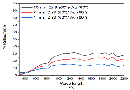
Further increase in deposition angle of Ag from ZnS(0)/Ag(30) to ZnS(0)/Ag(60) Figure 3 (c), decreased the reflectance. However, the nanostructure response to reflectance was not so sensitive to the small increase in deposition angle of silver metal films. The reduction in reflectance according to Liedtke et al., [43] was attributed to atomic shadowing that created areas with reduced grain size of silver atoms. This created imperfections in the Ag films. These imperfections generate grain boundaries in the thin films that decreased the reflectance of the thin films. As the number of grain boundaries increases with deposition angle, there is reduction in specular reflection for very thin films due to scattering of incident light. The increase in reflectance at wavelengths \(\lambda > 800\) nm was related to the increase of the Drude-like absorption in which the amount of voids in the metal phase increases [46].
The reflectance of obliquely deposited ZnS(30)/Ag(0) films presented in Figure 4 (a), can be described from two perspectives. Thus, the reflectance decreased with decrease in film thickness but also the reflectance increased along with the increase in wavelength of electromagnetic radiation.
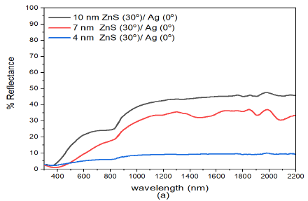
On the other hand, the deposition angle of ZnS had little impact on reflectance in the visible wavelength. The reflectance values in the visible region at about \(\lambda=800\) nm were 25.2% for (10 nm)ZnS(30)/Ag(0), 18.8% for (7 nm)ZnS(30)/Ag(0) and 6.4% for (4 nm)ZnS(30)/Ag(0) samples. However, the reflectance in the infrared wavelength decreased with increase in deposition angle of zinc sulphide. At about \(\lambda =1800\) nm, the reflectance values were 45.8% for (10 nm)ZnS(30)/Ag(0), 37.0% for(7 nm)ZnS(30)/Ag(0) and 9.4% for (4 nm)ZnS(30)/Ag(0) samples. This implies that increasing the deposition angle of ZnS increased the optical absorption in the infrared spectral region.
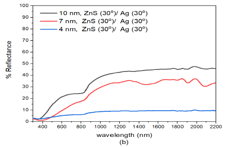
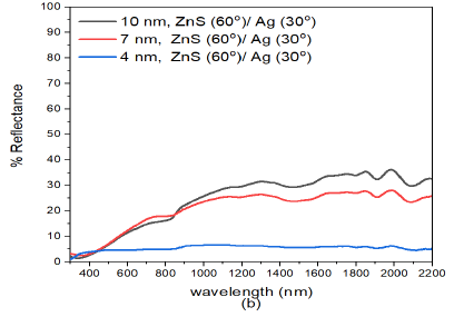
Reflectance of the samples in Figure 4 (b) decreased with decrease in film thickness of the ZNS/Ag composite. When the deposition angle of Ag was increased from (ZnS(30)/Ag(0) to (ZnS(30)/Ag(30), the reflectance of the multilayer was further reduced. This decrease was observed both in the visible wavelengths at about \(\lambda=800\) nm was as follows: 24.0% for (10 nm)ZnS(30)/Ag(30), 17.0% for (7 nm)ZnS(30)/Ag(30) and 6.3% for (4 nm)ZnS(30)/Ag(30). The reflectance values obtained in the infrared wavelengths at \(\lambda=1800\) nm were 45.1% for (10 nm)ZnS(30)/Ag(30), 36.5% for(7 nm)ZnS(30)/Ag(30) and 9.5% for (4 nm)ZnS(30)/Ag(30) specimens. The reflectance values in the infrared region were higher than those in the visible region. The reflectance of (4 nm)ZnS(30)/Ag(30) was exceptionally very low. This was largely contributed by the small film thickness, the oblique deposition angle of ZnS and silver thin films and optical absorption by the discontinuous islands of silver formed on glass substrate.
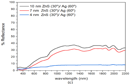
However, as the deposition angle of both ZnS and Ag was increased to ZnS(30)/Ag(60) Figure 4 (c), the reflectance of (10 nm)ZnS(30)/Ag(60), (7 nm)ZnS(30)/Ag(60) and (4 nm)ZnS(30)/Ag(60) further decreases with film thickness. The reflectance of (10 nm)ZnS(30)/Ag(60) and (7 nm)ZnS(30)/Ag(60) samples increased with increase in deposition angle of Ag. The reflectance of (4 nm)ZnS(30)/Ag(60) was extremely low at an average of \(< 3%\) in the visible region and \(< 5%\) in the infrared wavelength.
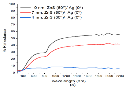
When the deposition angle of Ag was increased from ZnS(60)/Ag(0) to ZnS(60)/Ag(30), (Figure 5 (b)), The reflectance of the samples increased with increase in film thickness. The reflectance values further decreased in the visible as follows: 18.3% for (10 nm)ZnS(60)/Ag(30), 16.6% for (7 nm)ZnS(60)/Ag(30) and 5.1% for (4 nm)ZnS(60)/Ag(30). In the infrared regions, reflectance reduced as follows: 37.7% for (10 nm)ZnS(60)/Ag(30), 27.4% for (7 nm)ZnS(60)/Ag(30) and 6.0% for (4 nm)ZnS(60)/Ag(30). Interference effects observed along the entire electromagnetic spectrum. This trend is not observed in the (4 nm)ZnS(60)/Ag(30) multilayer film and its reflectance values are below 6% in the visible region. Interference effects were observed to diminish since much of the light was either absorbed or transmitted by the ZnS/Ag multilayer nanostructures.
The reflectance of the obliquely deposited ZnS(60)/Ag(60) samples decreased with decrease in film thickness as shown in Figure 5 (c). The increase in deposition angle of silver further decreased reflectance in the visible region. Interference effects are intense in the (10 nm)ZnS(60)/Ag(60), (7 nm)ZnS(60)/Ag(60) and (4 nm)ZnS(60)/Ag(60) nanostructures. The reflectance values in the visible wavelength for (10 nm)ZnS(60)/Ag(60), (7 nm)ZnS(60)/Ag(60) and (4 nm)ZnS(60)/Ag(60) mulitlayers were 17%, 13.7% and 10.5% respectively. In the infrared region, the reflectance of (10 nm)ZnS(60)/Ag(60) and (7 nm)ZnS(60)/Ag(60) nanolayers increased to 31% and 25.1% respectively.
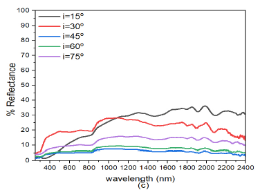
When the deposition angle of ZnS was increased from ZnS(0)/Ag(0) to ZnS(30)/Ag(0) Figure 6 (b), there was a slight decrease in reflectance both in the visible and infrared wavelength. This implies that increasing the deposition angle of ZnS decreased the reflectance of the ZnS/Ag nanofilms. Comparatively, these results were lower than those obtained in Figure 6 (a). At \(\lambda = 720\) nm, the peak reflectance values at \(i=30^o, 45^o, 60^o\) and \(75^o\) were 28.0%, 59.7%, 22.9%, 21.8%, and 17.0% respectively. Reflectance then started to increase at \(\lambda=800\) nm towards the infrared spectral region. Very strong interference effects were observed in the infrared region.
Further increase in the deposition angle of ZnS from ZnS(30)/Ag(0) to ZnS(60)/Ag(0) Figure 6(c), the reflectance values increased from the visble wavelength towards the infrared wavelengths. The reflectance peaks moved toward the short wavelength. At \(\lambda = 660\) nm, the peak reflectance values for \(i= 30^o\), \(45^o\), \(60^o\) and \(75^o\) were 29.2%, 59.7%, 22.9%, 21.8% and 17.0% respectively. After these peak values, there was a drop in reflectance at the upper edge of the visible spectrum. The reflectance values increased from \(i= 15^o\) to \(i= 30^o\). The reflectance then decreased from \(i= 45^o\) to \(i= 75^o\). The reflectance of visible light for which the angle of incidence \(i=30^o\), had a maximum value of about 59.7% at wavelength, \(\lambda=660\) nm. After this point, reflectance then dropped to about 46% at wavelength \(\lambda=883\) nm and it then increased progressively to about 82% at \(\lambda=2400\) nm. The reflectance for \(i=15, 45, 60\) and \(75^o\) in the visible region was quite different from the reflectance whose angle of incidence was \(i=30^o\). However, in the infrared region the the reflectance values did not differ so much as the wavelength increased. The low reflectance values revealed that the specimens ware transparent to visible light but highly reflective to infrared light. The interference effects in the infrared region (\(\lambda > 800\) nm) ware minimal compared to those obtained in Figure 6 (b).
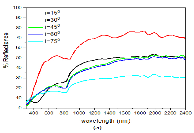
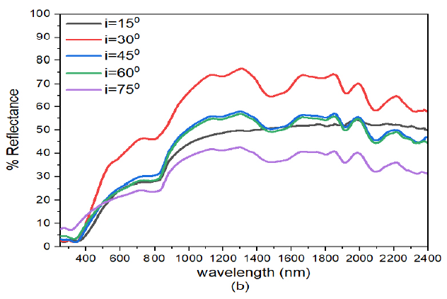
On increasing the angle of deposition of ZnS from ZnS(0)/Ag(30) to ZnS(30)/Ag(30) (Figure 7 (b), the reflectance values in the visible region was \(< 27%\). The spectra for \(i= 15^o\) had higher values in the visible wavelength followed by \(i= 30^o\). The spectra for \(i= 30^o\) had high reflectance values (62.7% at \(\lambda=2400\) nm) in the infrared wavelength. Other spectra had peak reflectance values in the range between 36.7% – 51.9% at 1979 nm. The reflectance decreased with increase in angle of incident radiation from \(i=15\) to \(45, 65\), and \(75^o\). Low values of reflectance in the visible region meant that this sample has reciprocally high transmittance values to visible light.
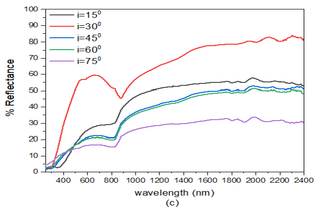
When the angle of deposition of ZnS was adjusted to \(60^o\) i.e. ZnS(60)/Ag(30), Figure 7 (c), reflectance values for different angles of incidence in the visible region were 28.0%, 59.5%, 22.4%, 21.3% and 17.2% for \(i=15^o, 30, 45, 65\), and \(75^o\) respectively. While the reflectance in the infrared region, reflectance values ranged between 36.4% – 57.9% for \(i=15^o\), 45.7% – 80.3% for \(i=30^o\), 22.3% -52.7% for \(i=45^o\), 20.5% – 51.2% – 51.2% for \(i=60^o\) and 16.1% – 34.0% for \(i=75^o\). The reflectance for \(i=30^o\) was higher than for \(i=15^o\) in the visible wavelength. This implies that this sample was transparent to both visible light and highly reflective to infrared light. The physical significance of this sample was that it could be used in applications involving antireflectors or in the reflection of thermally energetic infrared radiation with tilted angles of incidence between for for \(i=15^o\) to \(i=30^o\).
The excitation of surface plasmons by an external electrical field results in charge polarization on the metal surface. At resonance point (point at which frequency of applied field is equal to frequency of waves from electrical excitation), surface plasmon resonance occurs which leads to strong absorption or scattering of incident light. Surface plasmon absorption bands of Ag are in the visible and near infrared spectral regions. This is very useful for technological applications. When Zinc sulphide nanoparticles are subjected to the external electromagnetic field, coherent oscillations (surface Plasmon resonance) of the conduction electrons also occurs [48]. Surface plasmon effects are however, affected by several factors which include frequency of incident radiation, film thickness and formation of atomic islands on the surface of the dielectric substrate. Notebly, film thickness and deposition angle present a profound effect on spectral properties of thin film nanolayers. It is against this simple background that the Authors were prompted to carryout a comparison between reflectance and transmittance measurements on the samples.
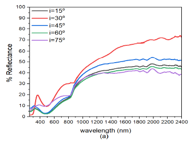
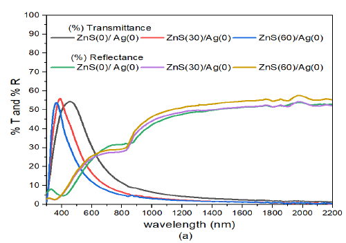
The transmittance spectra of (10nm)ZnS/Ag decreased with increase in deposition angle of ZnS in the wavelength range between (480 nm – 1200 nm), Figure 8 (a). In the wavelength range of 380 nm – 520 nm, the transmittance values were between 48% – 56%. The high transmittance of ZnS/Ag nano multilayers was due to high refractive index of ZnS that enhanced antireflection of incident electromagnetic radiation [49] and [50]. In the infrared region, at about \(\lambda = 800\) nm, the transmittance was \(< 20%\) and then the transmittance decreased rapidly as the wavelength was increasing. In the visible region, reflectance values were low ranging between 5% to 32%. The reflectance in the infrared wavelength increased from \(\lambda\) =800 nm to 2200 nm to a reflectance value of 58% at \(\lambda =\) 2000 nm.
The high transmittance in the visible spectrum is due to small thickness and relative homogeneity of the thin films at normal deposition angle of silver [51]. From the graph, there exist points which the researchers have referred to as equivalence points. These are points at which transmittance curves intersect the reflectance curves. These points occur in the wavelength range \(\lambda=570 – 640\) nm. High reflectance in the infrared region signifies poor transmittance to thermal infrared radiation while the same samples have relatively average values values to transmittance of visible light.
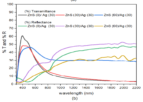
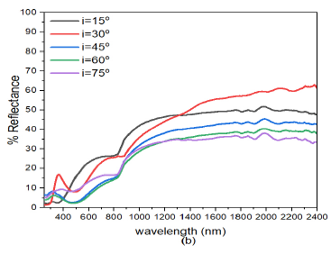
The transmittance of the deposited films decreased with increase in deposition angle of ZnS in the ZnS/Ag multilayer film in the visible region, Figure 8 (b). However, in the infrared region, transmittance increased with increase in deposition angle of ZnS. The reflectance in the infrared wavelength decreased with increase in deposition angle of ZnS films. The equivalence point were shifted and spread in the wavelength between 620 – 830 nm. This behaviour was also been reported in a recent study by [52].
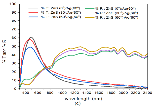
At high deposition angle of Ag i.e. ZnS/Ag(60) Figure 8 (c), the transmittance in the visible region increased considerably. However, transmittance decreased with increase in deposition angle of ZnS in the visible wavelengths. The transmission peaks at the wavelength of about 500 nm decreased with increase in deposition angle of ZnS. Where us in the infrared region, transmittance increased with deposition angle of ZnS. This shifted the equivalence point to about \(\lambda= 780\) nm. The physical shift in equivalence wavelength was due to high deposition angle of both zinc sulphide and silver films. The high deposition angle of Ag decreased the reflectance in the infrared region.
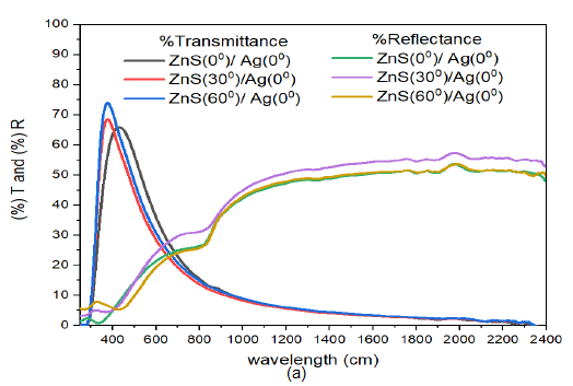
Additionally, reflectance increased from visible wavelengths to near infrared region of electromagnetic spectrum. These results were so close in the infrared region. Though the deposition angle for ZnS was increased from \(0^o\) to \(60^o\), the spectral response to deposition angle of ZnS did not change much. This shows that Ag nanoparticles strongly influence the transmittance and reflectance of the ZnS/Ag multilayer films. The reflectance of the samples in the visible region (\(\lambda =400-800\) nm) was low and ranged between 24% – 31% for the three deposition angles of ZnS. Reflectance in the infrared region for \(\lambda \geq 800\) nm was fairly good (between 55% and 58%). The transmittance in the visible spectrum was above average and ranged between 65% and 75% , Figure 9 (a).
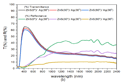
When the angle of deposition of Ag was increased from ZnS/Ag(0) to ZnS/Ag(30) (Figure 9 (b)), the transmittance in the visible region increased with increase in deposition angle of ZnS. The transmission peaks in the visible spectrum were obtained at around \(\lambda = 421\) nm with the following transmittance values: 65% for ZnS(0)/Ag(30), 63% for ZnS(30)/Ag(30) and 60% for ZnS(60)/Ag(30). The transmittance decreased progressively from 34.4% at \(\lambda= 800\) nm to 16.8% at \(\lambda = 2400\) nm. The reflectance in the visible region at \(\lambda =800\) nm was very low (ranged between 6.5% – 22.2%) and decreased with increase in deposition angle of ZnS. The reflectance then increased toward the near infrared spectral region. Interference effects decreased with increase in deposition angle of ZnS. Further analysis of Figure 9 (b), revealed that the transmittance values were very close in the entire electromagnetic spectrum. This meant that the changes in deposition angle of ZnS had less impact on the optical transmittance of the electromagnetic radiation. In the infrared spectral wavelengths, the reflectance values for ZnS(0)/Ag(30) and ZnS(30)/Ag(30) were greater than the transmittance of ZnS(0)/Ag(30), ZnS(30)/Ag(30) and ZnS(60)/Ag(30). The equivalence points were located at around 886 nm and 1054 nm in the infrared spectral wavelength.
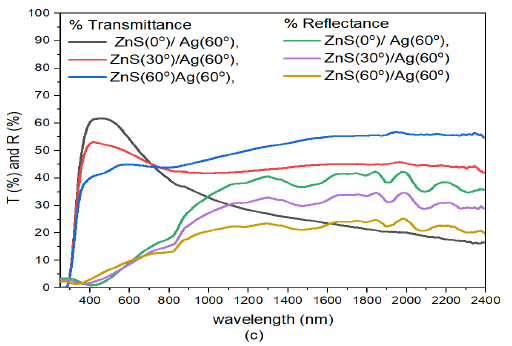
When the deposition angle of Ag nanoparticles in the composite was raised to \(60^o\) i.e. from ZnS/Ag(30) to ZnS/Ag(60) Figure 9 (c), there were remarkable spectral characteristics both in the visible and infrared wavelengths. The transmittance in the visible wavelength decreased with increase in the deposition angle of ZnS. The transmission peaks were observed in the wavelength range of 400 nm to 560 nm. The transmission peaks for specimen ZnS(0)/Ag(30), ZnS(30)/Ag(60) and ZnS(60)/Ag(60) were at 62.0%, 53.3% and 45.0% respectively. At about \(\lambda = 734\) nm, the trend in transmittance changed towards the infrared spectral range. The transmittance increased with increase in deposition angle of ZnS. This implies that the samples were more transparent to infrared radiation at high deposition angles of ZnS. Nevertheless, the transmittance of ZnS(60)/Ag(60) in the infrared wavelength was higher than the transmittance in the visible region by 11%. The reflectance spectra in the visible had low values of 18.6%, 15.6% and 13.6 for specimen ZnS(0)/Ag(30), ZnS(30)/Ag(60) and ZnS(60)/Ag(60) respectively at \(\lambda =\)800 nm. The reflectance then increased toward the infrared region but dependent on deposition angle of ZnS. The reflectance decreased with increase in deposition angle of ZnS and reflectance interference effects were observed in the infrared wavelength. High values of reflectance were obtained at \(\lambda = 1843.9\) nm and they were as follows: 43.5%, 34.9% and 25.0% for ZnS(0)/Ag(30), ZnS(30)/Ag(60) and ZnS(60)/Ag(60) respectively.
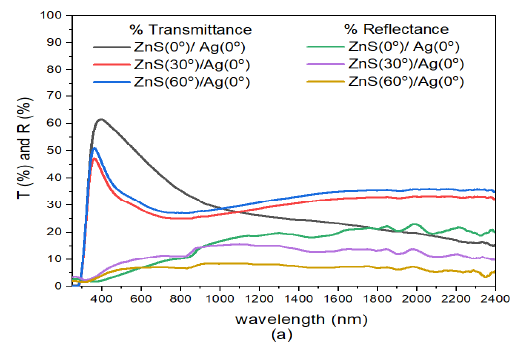
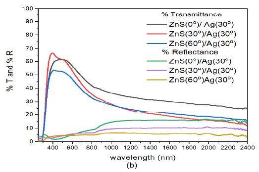
When the deposition angle of Ag nanoparticles was increased to \(30^o\), Figure 10 (b) the transmittance in the visible region increased with increase in deposition angle of Ag. However, the transmittance decreased with increase deposition angle of ZnS. The transmission peaks progressively moved toward the infrared wavelength of the electromagnetic spectrum. The recorded peaks in transmittance were 62.0%, 66.8%, and 53.5% for ZnS(0)/Ag(30), ZnS(30)/Ag(30) and ZnS(60)/Ag(30) respectively. At around \(\lambda =1072\) nm, the transmittance tends to increase with the deposition angle of ZnS. Nevertheless, the transmittance of ZnS(0)/Ag(30) remained relatively high. The reflectance values in the visible were low ranging between 3% – 9%. A slight increase in reflectance was observed at 803 nm. However, the reflectance decreased with increase in deposition angle of ZnS. Highest reflectance in the infrared region was obtained at \(\lambda = 1985\) nm as follows: 16.3% for ZnS(0)/Ag(30), 11.2% for ZnS(30)/Ag(30) and 6.1% for ZnS(60)/Ag(30). The reflectance values were generally lower than the transmittance values. These samples were transparent to infrared and visible light wavelengths. However, they might not be suitable for thermal infrared control applications.
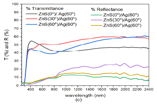
When the deposition of Ag nanoparticles was increased further to \(60^o\) i.e. ZnS(30)/Ag(60) 10 (c), transmittance of the samples in the visible region decreased with increase in deposition angle of ZnS. The transmission peaks in the visible were located between 381 – 580 nm. The peak values for transmittance in this region were 55.0%, 51.5% and 45.3% for specimen ZnS(0)/Ag(30), ZnS(30)/Ag(30) and ZnS(60)/Ag(30) respectively. The transmittance values in infrared wavelength were higher than those in the visible region. The reflectance of the samples was very low and ranged between 3.3% – 10.3% in the wavelength range 383 – 780 nm. At around 800 nm, the reflectance increased towards the infrared wavelengths. Highest reflectance was obtained at wavelength of 1983 nm for different specimens. The reflectance values obtained were as follows: 10.1% for ZnS(0)/Ag(30), 27.3% for ZnS(30)/Ag(30) and 15.5% for ZnS(60)/Ag(30). The transmittance values were generally higher than the reflectance values in the entire electromagnetic spectrum. The significance of these results implies that these specimens are not desirable for use in thermal infrared control and anti-reflection applications.