
Crosstalk noise is a critical signal integrity constraint in highly scaled ICs due to reduced spacing between interconnects and low supply voltages/noise margin. Evaluation of the impact of noise and methods to guarantee switching in the presence of thermal/electrical stress become necessary in modern high-density logic [1,2]. In particular, the issue becomes more critical in fast digital blocks and dynamic receivers where any small disturbance on an input can be amplified by subsequent logic gates [3–5].
The scaling of interconnect leads to increased resistivity and capacitive coupling. Reduced metal width results in increased line resistance, and increased thickness required to compensate for increased resistivity leads to increased sidewall capacitance, and hence to the formation of the RC-network with high sensitivity of a victim interconnect to any changes in aggressor interconnect. Second factor which can lead to excessive crosstalk noise level is the temperature variation since increased metal resistivity and decreased carrier mobility will degrade the capability of the victim driver to hold logic value [6,7].
The thermal effects in terms of interconnect delay and noise have been analyzed for traditional RC-coupled interconnects, graphene nanoribbon interconnects, and carbon-nanotube bundle interconnects [7–11]. Temperature compensation circuits were proposed to deal with temperature-related delay uncertainty [12]. However, although there is an understanding that temperature influences the performance of interconnects, the need for suppression of additional noise, arising due to high temperature only and making the victim logic to fail, has not yet been met with a circuit-level solution. The research question which this work tries to answer is whether it is possible to use a local small circuit to filter out such an additional thermal effect on the crosstalk noise in order to avoid driver sizing.
In this work, the increase in switching crosstalk from \(25^{\circ}\mathrm{C}\) to \(125^{\circ}\mathrm{C}\) in 22 nm CMOS interconnects is estimated. The term TICN (Temperature Induced Crosstalk Noise) is defined as an additional high-temperature component of the victim disturbance, and it is analyzed whether PTAT/CTAT-generated gate biases of the TG can help to filter out this component in the case of a six-stage inverter receiver. The contribution of this work is a temperature-controlled TG filter which allows increasing the PMOS gate voltage \(V_{GP}\) with temperature rise and decreasing the NMOS gate voltage \(V_{GN}\) with temperature rise.
There are plenty of VLSI applications where on-chip temperature can reach high values due to high power density and/or necessity to operate in the whole temperature range up to \(125^{\circ}\mathrm{C}\) [12,13]. Thus, it becomes necessary to consider the possibility to locally suppress the crosstalk noise in a thermally nonuniform chip.
Propagation delay for a CMOS gate is usually modeled as a function of load capacitance, supply voltage, and drain current in terms of an alpha power law form [14]. For a driver connected to a load capacitance of \(C_L\), the delay variation is modeled by
where \(V_{DD}\) is the supply voltage, \(I_D\) is the drain current, \(\mu(T)\) is the temperature dependence of the carrier mobility, \(V_{TH}(T)\) is the temperature dependent threshold voltage and \(\alpha\) is the velocity saturation parameter of the technology used.
Both \(\mu(T)\) and \(V_{TH}(T)\) are affected by temperature variations. Increase in temperature decreases carrier mobility resulting in lower drive current. On the other hand, increase in temperature results in lowering of threshold voltage resulting in increase in current. At a nominal supply voltage of 0.8 V for 22 nm technology, mobility variation dominates the victim driver characteristics. Hence, the restoring capability of the victim driver operating at higher temperatures will be weak to control a coupling induced disturbance.
The inductive term is negligible for the RC interconnect model analyzed in this study. Also, the temperature effect on capacitance is significantly lower than the one of the temperature on the resistance of the interconnect. Therefore, the most significant temperature effect in the studied case is the increase in metal resistance. The temperature-dependent model of the resistance of the interconnect segment has the form [7]:
where \(R_0\) is the resistance of the interconnect segment at nominal temperature \(T_0\), \(\alpha_R\) is the temperature coefficient of the resistance, and \(T\) is the temperature of the wire. The combination of an increase in the interconnect resistance and a decrease in the victim driver strength explains why the crosstalk disturbance is higher at \(125^{\circ}\mathrm{C}\) than at \(25^{\circ}\mathrm{C}\).
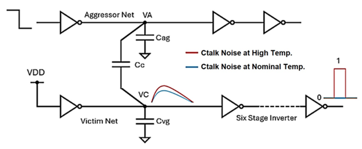
The thermally induced switching crosstalk noise is examined using two adjacent signal nets. The switching net is called the aggressor, while the net that is subject to the influence of the capacitive coupling is called the victim. There is a coupling capacitance \(C_c\) between these nets. On the other hand, the victim net is connected to a six-stage inverter chain that models the receiving logic.
In the positive-glitch case shown in Figure 1, the output node of the aggressor \(V_A\) rises while the victim node \(V_C\) is held close to the logic zero value. Switching the voltage creates the displacement current in the coupling capacitance \(C_c\) that increases the value of \(V_C\). At the nominal temperature, the disturbance dissipates before propagating through the receiver logic. With the high victim temperature, the same aggressor transition causes greater disturbance due to the increased resistance of the victim driver and interconnect. A pulse below the threshold of the inverter is filtered out, while the pulse above the inverter switching threshold propagates through as the erroneous logic event [5,15].
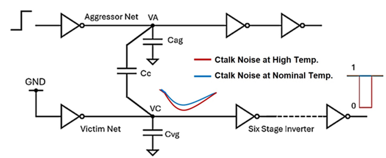
The complementary case illustrated in Figure 2 takes place if the aggressor transition drops the victim node from the state where it is held in the logic-one state. In this case, the polarity is changed but the implication for the reliability is the same: the higher the temperature of the victim, the more likely the disturbance reaches the logical threshold of the receiver. Two mentioned cases prove that TICN is not limited to one switching direction; it is a temperature-dependent degradation of the noise margin of both rising and falling coupled transitions.
The simulation was done using the 22 nm bulk CMOS technology with the global interconnect parameters obtained from the Table 1 [16]. The HSPICE simulations were conducted using the PTM devices with \(V_{DD}=0.8\) V [17]. Although the process variation is not the main subject of the analysis, it should be noted that there are significant sensitivities of nanometer circuits to the device and interconnect parameter variations. Therefore, using the technology-consistent models of the devices is justified [15]. The two coupled wires in the circuit are implemented using the distributed \(6\)-\(\pi\) RC network shown in Figure 3 [18].
| Dimensions | Local/Intermediate | Global |
|---|---|---|
| Pitch \((w+s)\) (nm) | 44 | 64 |
| Width \(w\) (nm) | 22 | 32 |
| Thickness \(t\) (nm) | 44 | 80 |
| Aspect ratio | 2 | 2.5 |
| Spacing \(s\) (nm) | 22 | 32 |
| Height \(h\) (nm) | 45 | 76.8 |
| Dielectric constant \(K\) | 2.55 | 2.55 |
| Resistivity (\(\Omega\) nm) | 60.1 | 42 |
Values in Table 1 reveal that while the global line has a bigger cross section compared to the intermediate line, its spacing is bigger too. All the values define the ratio between the ground capacitance and the lateral capacitance. The reason is that being long, the global line is affected by the RC values.
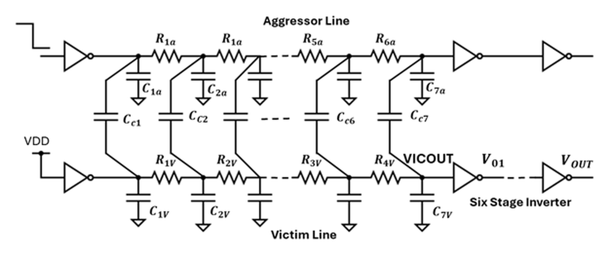
The ground capacitance \(C_g\) and coupling capacitance \(C_c\) are calculated from the interconnect geometry according to [19]
The resistance of a wire segment is calculated as
where \(\rho\) is resistivity, \(L\) is the wire length, \(w\) is wire width, and \(t\) is wire thickness.
The extracted values from Table 2 indicate that the value of the coupling capacitance is much larger than the value of the ground capacitance in the chosen global line structure. The high ratio of the coupling capacitance is responsible for the victim waveform being strongly dependent on the transition of the aggressor.
| Ground capacitance \(C_g\) (nF/m) | Coupling capacitance \(C_c\) (nF/m) | Resistance \(R\) (k\(\Omega\)/m) |
|---|---|---|
| 18.34 | 52.37 | 16.4 |
Thermally induced crosstalk noise (TICN) is characterized as the extra voltage crosstalk caused by increasing temperature of the victim line keeping the nominal-temperature aggressor transitions unchanged:
Here, \(V_{\mathrm{xtalk}}\) is the signal measured at the victim’s receiver input, which is the input of the six-stage inverter chain in our experiments. Note that the choice of the sign in Eq. (6) means that TICN will be positive if the crosstalk in the high-temperature case leads to a higher disturbance than the nominal-temperature case.
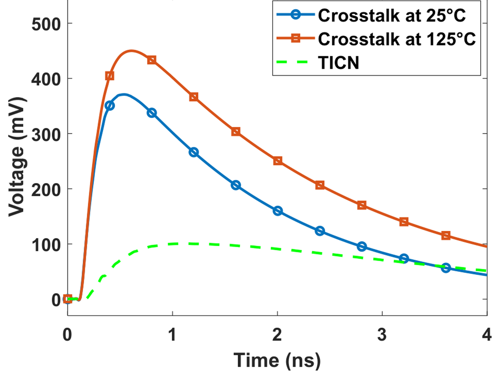
The effect of increasing crosstalk for all aggressor strengths is demonstrated by the driver-size sweep in Figure 4. The additional green bars correspond to the thermally induced component. One can see that the thermal increase is essential for the cases where the nominal disturbance is closer to the receiver threshold. In such cases, a small thermal increment may turn an attenuated glitch into the propagating error.
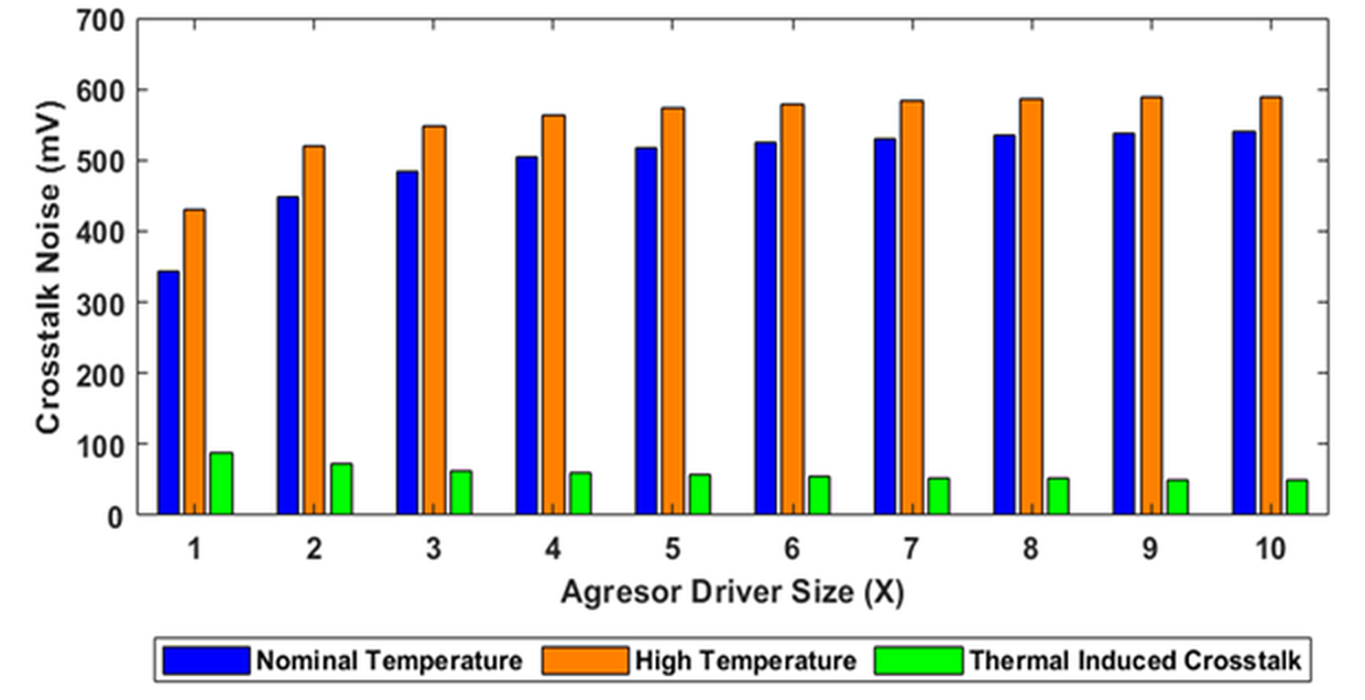
Figure 5 illustrates this transition to the switching regime. For 2X aggressor driver, the nominal-temperature victim crosstalk equals 363.8 mV, while the victim crosstalk at \(125^{\circ}\mathrm{C}\) rises to 444.5 mV. As a result, TICN reaches 80.7 mV. It is a significant additional voltage considering that the supply voltage is 0.8 V since the inverter switching threshold is close to its half.
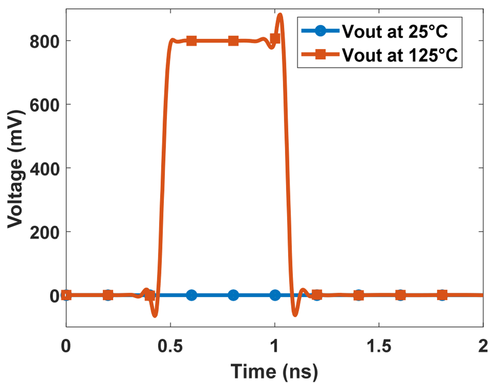
Receiver Output of Figure 6 proves that the TICN component is having a functional consequence. At \(25^{\circ}\mathrm{C}\), the victim input disturbance does not cause switching of the six-stage inverter chain and \(V_{OUT}\) stays at its intended value. On the other hand, at \(125^{\circ}\mathrm{C}\), the victim disturbance, after getting amplified, crosses the effective threshold causing propagation of error to the chain, thereby resulting in erroneous output switching. Hence, TICN must be considered as a circuit-level reliability issue.
Pass transistor and transmission-gate-based circuits have been utilized for mitigation of transient pulses and protection from soft error susceptibility [20–22]. Conventional TG remains always on since the gate terminal of the PMOS is tied to ground and NMOS gate is tied to \(V_{DD}\). While such arrangement allows passing data with minimum resistive load, the filtering ability of TG cannot be dynamically adjusted in response to temperature-related variations in crosstalk magnitude.
TICN suppressing circuit employs TG located in line with the victim-line receiver input and preceding six-stage inverter chain as illustrated in Figure 7. The gate of NMOS pass transistor is set to voltage \(V_{GN}\) while the gate of PMOS pass transistor is set to \(V_{GP}\). As the temperature grows, both voltages are adjusted so that TG filters the growing crosstalk pulse at higher temperature while allowing passing any valid transitions. Such insertion location is crucial since the pulse is filtered out prior to being regenerated by the highly gainful receiver stages.
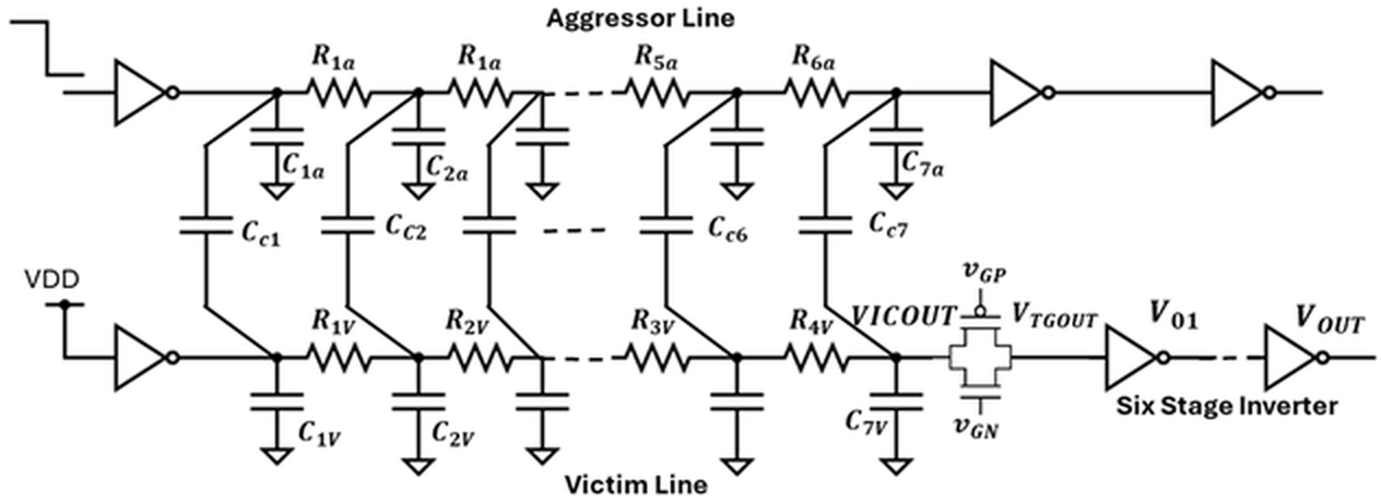
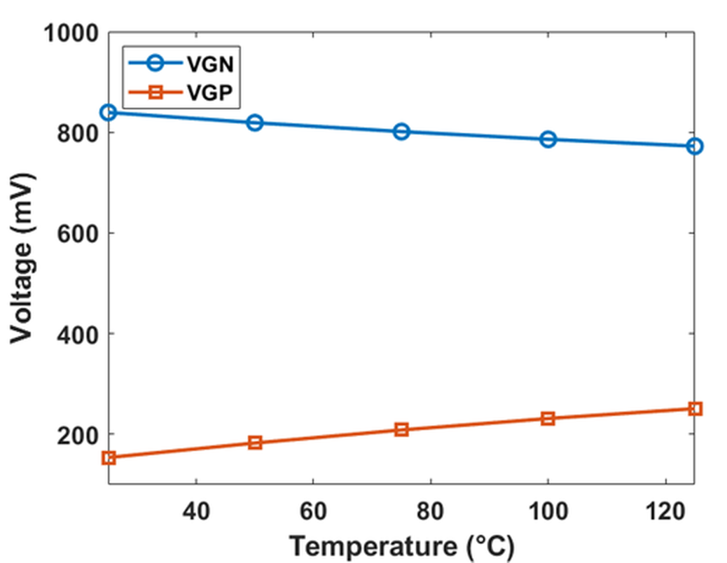
Table 3 shows gate bias voltages required for four temperatures. It can be seen that NMOS gate voltage \(V_{GN}\) decreases with increase of temperature, while the PMOS gate voltage \(V_{GP}\) increases. The reverse polarity change in voltage values leads to controlled decrease in pass transistor strength which enhances pulse filtering as TICN contribution grows.
| TG gate voltage | \(50^{\circ}\mathrm{C}\) | \(75^{\circ}\mathrm{C}\) | \(100^{\circ}\mathrm{C}\) | \(125^{\circ}\mathrm{C}\) |
|---|---|---|---|---|
| \(V_{GN}\) (mV) | 840 | 820 | 760 | 740 |
| \(V_{GP}\) (mV) | 160 | 180 | 240 | 260 |
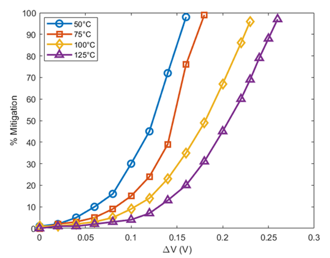
The mitigation profile shown in Figure 8 illustrates the effect of the voltage change on crosstalk suppression. When the temperature is lower than around \(65^{\circ}\mathrm{C}\), the crosstalk pulse will be below the switching threshold without the need for any strong filtering. When the temperature rises up to \(75^{\circ}\mathrm{C}\), the \(\Delta V\) required is around 140–180 mV. For temperatures of \(100^{\circ}\mathrm{C}\) and \(125^{\circ}\mathrm{C}\), the needed range of \(\Delta V\) is around 200–240 mV and 230–260 mV, respectively. The monotonic relationship with temperature proves that the TG is not supposed to be biased at any fixed point.
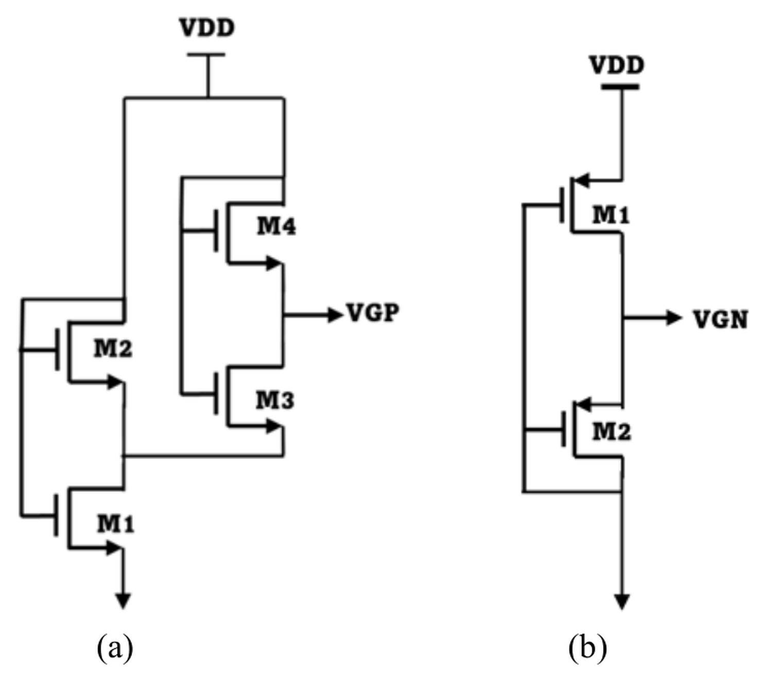
The gates voltages can be provided using the circuits of the temperature sensors illustrated in Figure 9. The PTAT circuit is used for providing the gate voltage \(V_{GP}\) of the PMOS, while the CTAT circuit provides the gate voltage \(V_{GN}\) of the NMOS. This task is ideally solved with the help of PTAT and CTAT biasing techniques since they allow obtaining the temperature value as a control voltage signal without any digital control [23,24].
The voltages generated in Fig. 10 have the same qualitative behavior as that of the TG control voltages. The behavior of \(V_{GN}\) voltage is a negative temperature coefficient since it decreases from the high voltage level to a lower gate voltage with increase in temperature. The behavior of \(V_{GP}\) voltage is a positive temperature coefficient since it increases from the low voltage level to a higher gate voltage with increase in temperature.
The performance of the suppression circuit has been tested through more than 500 HSPICE simulations with respect to interconnect length varying between 700 and 1000 µm, coupling length ranging between 300 and 800 µm, aggressor driver size varying from 5X to 20X, and victim driver size varying from 1X to 3X. In all cases, the average percentage decrease in TICN is 96% while in 87% of the total number of cases the thermal effect has been successfully canceled. This implies that the failure due to the main cause of failure at high temperatures can be corrected at the receiver input without having to modify the aggressor and victim driver dimensions.
The exemplary cases from Table 4 show the conditions under which the TG works efficiently. Out of the fourteen examples, eleven cases eliminate entirely the thermally-induced portion of the problem, bringing the crosstalk mitigated at \(125^{\circ}\mathrm{C}\) back to the nominal value or even slightly below it. In all other cases, the TG eliminates 65%, 87%, and 91% of the thermal effect. This occurs due to the effect of the combination of driver strength and shorter coupling length on the pulse shape which cannot be eliminated by the TG chosen bias.
In addition, it is evident from the results that the magnitude of high-temperature crosstalk is not the only factor contributing to the difficulty in mitigating the crosstalk problem. For instance, the crosstalk instances of 125 degreeC above 600 mV are completely mitigated when the TG bias is consistent with the pulse duration and receiver threshold, while some instances of smaller magnitude still have a residual part. Thus, it can be concluded that the TICN suppression is dependent on both amplitude and the pulse width. A TG at the receiver side is thus useful because it reduces the waveform just before the logic regeneration.
Design-wise, the key result is that there is no resizing of the driver itself in the circuit. While resizing the victim driver could help achieve improved noise immunity, this would result in an increase in area, input capacitance, dynamic power, and might affect timing closure as well. The temperature-dependent TG, on the other hand, applies the filter locally to the receiver input, and does so selectively, when the temperature increases. This enables the approach to be used in situations where there are spatially non-uniform temperature profiles, whereby only some receivers around hotspots require extra suppression.
In this research, the ability to suppress thermal crosstalk noise arising in nano-scale CMOS interconnects using a small local circuitry without scaling up interconnect drivers was investigated. It was found that high victim temperature could raise a harmless crosstalk signal into a level that could flip a six-inverter receiver stage. With 2X aggressors, the disturbance experienced by the victim rises from 363.8 mV at \(25^{\circ}\mathrm{C}\) to 444.5 mV at \(125^{\circ}\mathrm{C}\), thus causing 80.7 mV TICN.
| Case | Driver size Agg./Vic. | (µm) interconnect/coupling | Switching crosstalk mV | TICN mV | After mitigation at \(125^{\circ}\mathrm{C}\) (mV) | TICN reduction % | |
|---|---|---|---|---|---|---|---|
| \(25^{\circ}\mathrm{C}\) | \(125^{\circ}\mathrm{C}\) | ||||||
| 1 | 10X/1X | 1000/600 | 571 | 636 | 65 | 569 | 100 |
| 2 | 10X/2X | 1000/700 | 527 | 603 | 76 | 520 | 100 |
| 3 | 10X/2X | 1000/600 | 504 | 578 | 73 | 498 | 100 |
| 4 | 10X/2X | 1000/800 | 545 | 622 | 77 | 544 | 100 |
| 5 | 10X/3X | 1000/600 | 470 | 543 | 73 | 477 | 91 |
| 6 | 10X/3X | 1000/700 | 491 | 566 | 76 | 491 | 100 |
| 7 | 10X/3X | 1000/800 | 507 | 585 | 78 | 505 | 100 |
| 8 | 20X/3X | 1000/700 | 503 | 578 | 75 | 496 | 100 |
| 9 | 20X/3X | 1000/400 | 422 | 487 | 65 | 444 | 65 |
| 10 | 20X/3X | 1000/500 | 456 | 525 | 70 | 465 | 87 |
| 11 | 20X/3X | 1000/600 | 483 | 555 | 72 | 480 | 100 |
| 12 | 10X/2X | 700/300 | 462 | 529 | 67 | 451 | 100 |
| 13 | 10X/2X | 700/500 | 590 | 668 | 77 | 585 | 100 |
| 14 | 5X/2X | 700/500 | 557 | 640 | 83 | 545 | 100 |
The temperature-controlled transmission-gate structure is designed specifically to mitigate this failure mode through the use of CTAT and PTAT gate biases for the NMOS and PMOS pass transistors, respectively. The temperature dependence of the \(V_{GN}\) and \(V_{GP}\) voltages tunes the TG attenuation according to temperature such that the high temperature portion of the crosstalk pulse is filtered out prior to reaching the receiving logic circuitry. Through simulation of over 500 different combinations of interconnect parameters and driver strengths, the circuit exhibits an average TICN reduction of around 96% and cancellation in 87% of the cases tested. The results show that temperature controlled local filtering is a viable and scalable solution to enhance signal integrity in 22 nm CMOS interconnects subject to thermal stress.
Acknowledgments: The authors acknowledge the use of circuit simulation tools and technology models that supported the analysis.
Author Contributions: Both authors contributed to the circuit analysis, interpretation of results, manuscript preparation, and approval of the final manuscript.
Conflicts of Interest: The authors declare no conflicts of interest.